|
|
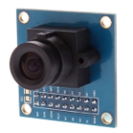
| Figure 2.1: OV7070 camera module (used
in this project). |
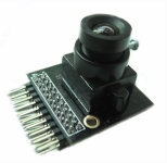
Figure 2.2: OV7070 + AL422 FIFO camera module. |
| Signal | Usage | Active |
|---|---|---|
| 3V3 | 3.3V power | |
| Gnd | Ground | |
| SIOC | Serial command bus clock (up to 400KHz) | |
| SIOD | Serial command bus data | |
| VSYNC | Vertical Sync | Active High, configurable |
| HREF | CE output for pixel sampling | Active High, configurable |
| PCLK | Pixel Clock | |
| XCLK | System clock (10-48MHz, 24MHz Typ) | |
| D0-D7 | Pixel data | |
| RESET | Device Reset | Active Low |
| PWDN | Device Power Down | Active High |
| C0 |
C1 |
C2 |
C3 |
|
| R0 |
0,0 |
0,1 |
0,2 |
0,3 |
| R1 |
1,0 |
1,1 |
1,3 |
1,3 |
| R2 |
2,0 |
2,1 |
2,2 |
2,3 |
 |
 |
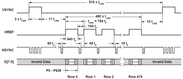
| Figure 2.5: VGA frame timing
(datasheet of OV7670 camera module). |
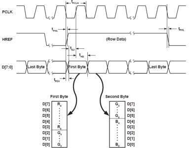
Figure 2.6: RGB 565 output timing diagram (datasheet of OV7670 camera module). |
| void read_a_frame_from_ov7670(void) { uint32_t i = 0; while (VSYNC); // wait for the old frame to end while (!VSYNC); // wait for a new frame to start while (VSYNC) { while (VSYNC && !HREF); // wait for a row to start if (!VSYNC) break; // row did not start, but frame ended while (HREF) { // wait for a row to end; // first byte while (!PCLK); // wait for clock to go high // get the first 8 bits, i.e., the first byte frame_buffer1[i] = LPC_GPIO2->FIOPIN; while (PCLK); // wait for clock to go back low // second byte while (!PCLK); // wait for clock to go high frame_buffer2[i] = LPC_GPIO2->FIOPIN; while (PCLK); // wait for clock to go low i++; } } } |
| Figure 2.7: Embedded C function to
receive two bytes of data (16 bits) for each of the pixels
of a frame. This code is written in the context of using the
LandTiger 2.0 board for which we write embedded C programs
using ARM Keil's IDE. Also, we work with VSYNC negative,
which can be set up by programming appropriately first the
camera's registers. |
 |
 |
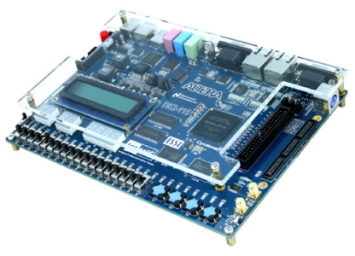
| Figure 2.8: DE2-115 FPGA board. |
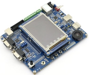
Figure 2.9: LandTiger 2.0 board. |
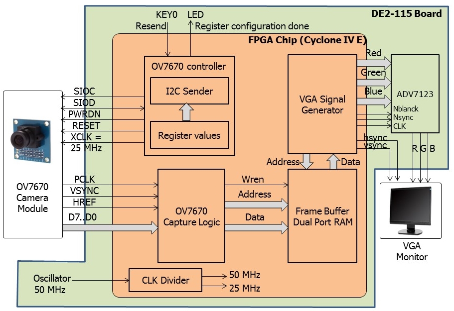 |
| Figure 3.1: Block diagram of project Implementation #1. |
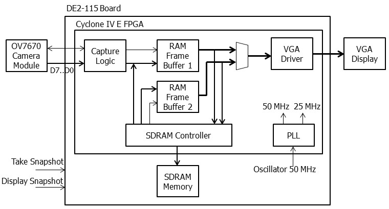 |
| Figure 4.1: Simplified block diagram of project Implementation #2. |
 |
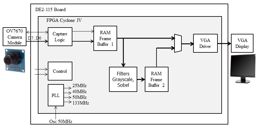
| Figure 5.1: Simplified block diagram of project Implementation #3. |
 |
| Figure 6.1: Simplified block diagram of project Implementation #4. |
 |
 |
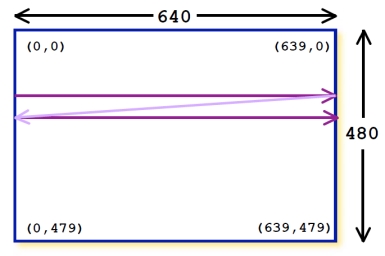
| Figure A.1: Scanning of a frame from pixel
0,0 to pixel 639,479. |
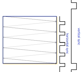
Figure A.2: Illustration of Vsync and Hsync signals. |